SITEMAP |  JAPANESE
TOP About Accverinos Product information Details of service Image of future concepts Contact Links Download

Top page>>Product information>>SDRAM module M-2

Revised October 2007


SDRAM module M-2
Memory module in which a 133MHz memory clock SDRAM can be mounted
Features    
   

- Memory module: 144-pin SO-DIMM 133 MHz, 256MB (up to 512 MB may be available).
- FPGA: Xilinx XC2V6000-FF1152 (XC2V8000-FF1152 also available).
- Up to 8 of M-2 modules can be mounted on B-1.
- Total 556 user I/Os.
- FPGA function DCI (digitally controlled impedance) may be available.
- Design Gateway configuration supports: FlashLink.
- Sample FPGA circuit core-IP (memory controller and PCI) and PC base software (Windows driver and application software) source code may be applied.

SDRAM photograph

Function block diagram    
   

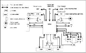
· The signals connected to CN1 - CN4 can all be user by the user.
· Clock input can be freely selected from among input from the base system (33MHz), OSC on the module (50MHz), SMA input, input from another module (CN1 - CN4), etc.
· Clock can be provided non-skewed to the SDRAM, FPGA by the clock driver on the functional module.
· Input and output to the base system (PCI, LED, SW, etc.) can all be used.
· LEDs are provided for debugging.

 
Function block diagram SDRAM

Sample IP core    
   

· SPD ROM writing function using I2C
· SDRAM initialization function
· 133MHz burst transmission function
· PCI target function
· Mapping memory on module to PCI memory space
· Test pattern generation circuit for test purposes
· I/O pins, DCM optimized for 133MHz

 
SDRAM Sample IP Core
 

>>For inquiries click here

 
Copyright©2007, Accverinos Co.,Ltd. All rights reserved.