 |
 |
 |
|
|
|
|
|
|
|
|
- Interfaces: PCI, signal monitoring
connectors, extension connectors, Switches, and LEDs.
- PCI bridge can be applied : PCI-bus of personal computer can be
connected to B-1 Base System.
- Dedicated signal lines (Clock, JTAG, Reset).
- Clock lines (there are two clock signal lines.):
· Peer-to-peer clock lines between neighboring functional
modules.
· Individual global clock signal lines for the separated
functional module block.
- JTAG chains, reset and control lines.
- Configuration scheme: All functional modules can be configured
by using JTAG-chain on B-1 Base System.
Stand-alone configuration also available.
- Each functional module connects to its own power source.
- B-1 Base System contains PLD reset control module and DC power
supply module for each functional module.
- Chassis: choose from metal type or acrylic type.
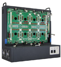
B-1 metal chassis
|
|
B-1 metal chassis with functional module mounted 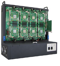 |
|
|
|
|
|
 |
|
|
|
|
|
|
|
B-1 has the following interfaces. All of these interfaces
are connected to functional modules, so users can utilize such interfaces
easily for their own circuit design.
· Connectors for mounting functional modules (*1)
· PCI(*2)
· IDE connector shape signal input and output connector
· Connector for logic analyzer (*3)
· Serial port
· Rotary switch
· DIP switch
· Push switch
· LED
*1 A maximum of 698 signals can be
connected to the functional modules.
A maximum of 698 signals can also be connected between adjacent
functional modules.
*2 By mounting a commercial PCI bridge card, the PCI bus on a personal
computer can be extended onto the B-1,
and it is possible to control the functional module from the personal
computer.
*3 Probes for a total of 32ch of multi-purpose logic analyzers can
be connected to the B-1.
Also, P6860 low capacitance active probes manufactured by Tektronix
Inc. can be connected.
|
Regarding clock wiring:
The B-1 clock wiring includes the following two systems.
1. Pear-to-Pear clock wiring between adjacent functional modules
Clock wiring between adjacent functional modules mounted on B-1.
The clock on one functional module is transmitted, and the clock is received by the other functional module.
With these clocks, 200MHz data transmission clocks can be achieved.
2. Common clock wiring between functional module block units
Wiring to provide clock from B-1 to functional module block units.
A common clock can be transmitted from B-1 to a maximum of 4 functional
modules.
If a PCI bridge is mounted on the B-1, the PCI clock provided from the personal computer can be transmitted to functional modules.
|
Regarding the PCI bridge function:
By mounting a PCI bridge card on the B-1, the PCI bus on a personal computer can be extended onto the B-1.
A commercial PCI bridge card is included with B-1 as standard configuration.
|
|
Regarding FPGA configuration:
The following 2 methods can be used for configuring FPGAs on B-1.
1. Method of configuring each functional module on B-1
A JTAG port is mounted on the B-1, and furthermore the JTAG chain
connection is provided, so that each functional module can be configured
at once.
Also, the JTAG chain can be switched ON/OFF in functional module units.
2. Method of configuring on functional modules
An FPGA dedicated configuration ports and JTAG port are provided
so that configuration can be carried out on each functional module.
Also, the commercial FlashLink (ROM for configuration) product is
included as standard.
* Writing data from FlashLink to an FPGA is completed in a few seconds, so this results in shorter debugging time.
|
Regarding power supply:
The necessary power supply is provided to each functional module from B-1 via a dedicated power supply harness.
In providing power, boot timing is controlled by the power supply ON/OFF control circuit of the reset circuit.
|
Regarding the reset circuit:
On the B-1, a PLD onto which the reset control circuit is written is mounted as a reset module.
Using the reset module, each power supply module is controlled ON/OFF, and individual functional modules
or all mounted functional modules can be reset.
|
Types of chassis and external power supply devices:
There are 2 types of chassis for supporting the B-1 that can be selected when placing an order.
1. Acrylic chassis
Chassis made of transparent acrylic resin.
2. Metal chassis
Chassis made of metal.
|
|
|
|
It is necessary for customers using an acrylic chassis to provide an external power supply (DC +5V output) (*4).
Customers using a metal chassis do not need to provide an external power supply.
An AC 100V power supply can be connected to the metal chassis.
*4 We can provide it for you as
your request.
|
|
 |
|
System bus connection diagram 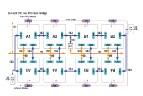
| Clock connection diagram 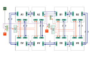
|
|
|
|
>>For inquiries click here
|
