|
- Memory module: two 200-pin SO-DIMM DDR 200/400
MHz, mounted on the surface and the back side.
Off-the-shelf PC3200 DDR memory module (for laptop PC)
can be used. *1)
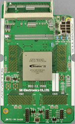
- FPGA: Altera Stratix II FPGA (EP2S130FF1508) *2)
- Up to 8 functional modules can be mounted on B-1 Base System.
- Total 730 user I/Os (excluding DDR memory module interface).
- Altera configuration cable supports; Byte Blaster II, Byte Blaster
MV, USB-Blaster and Master Blaster serial/USB Communication Cable
Altera configuration cable
- Design Gateway configuration supports: FlashLink and JtagLink
|
 |
|
|
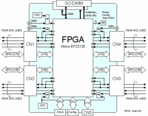
· CN 1-4 for connecting to the base system
and I/O for connecting to CN5 for connecting to multi-purpose I/O
can all be used by the user.
CN 1/4 include 175 multi-purpose I/Os, and there are 2 each for
dedicated clock input/output, to give a total of 179.
CN 2/3 include 176 multi-purpose I/Os, and there are 2 each for
dedicated clock input/output, to give a total of 180.
CN 5 includes 12 multi-purpose I/Os. CN 1-4, 5 have a total of 718
I/Os.
· 2 OSCs can be mounted for each of DDR memory and the system
clock. 3 SMA connectors can be mounted for external clock input.
· Clock input to modules include 2 each to CN 1-4, and the
clock for DDR memory, to give a total of 9. These can be freely
selected as input from the module base system, external input via
OSC, SMA connectors on the module, or input from another module,
etc.
· The 2 DDR memories mounted on the module and FPGA are connected
by the data bus (DQ/DQS) as a common signal. Other addresses, blocks,
and control lines are connected independently.
· All the inputs and outputs of the base system (PCI, LED,
DIP-SW, ROT-SW, etc.) can be used.
· FPGA's I/O power supply voltage value can be changed by
jumpers on the board. The standard configuration is 2.5 Volts.
|
|
|