|
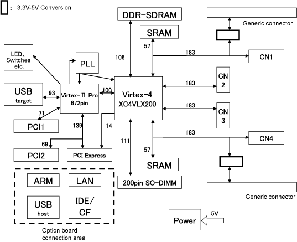
- DDR memory module: 200-pin SO-DIMM PC2700 (166/333
MHz), 512 MB, fast SRAM, 16 M-bits.
- On-board memory: PC2700 (166/333 MHz) DDR memory, 512 MB.
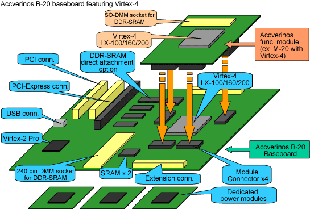
- FPGA: Xilinx Virtex-4 XCE4VLX100/160/200-FF1513.
- Interface: USB 2.0 and PCI.
- Accverinos series functional module can be mounted (Data transfer
speed between B-20 and the functional module is assured up to 200
MHz).
- Maximum 2M ASIC gate count circuit (when using XCE4VLX200 and
M-20 functional module).
- Flexible connectivity by using PCI board or custom interface board.
- Chain connectivity with multiple B-20 Base Systems.
- Gated-clock can be realized on B-20 Base System.
- Micro ATX Chassis (easy to use).
- Sample FPGA circuit core-IP (memory controller) and PC base software.
- Sample software (Windows driver and application software) supplied
as source code.
|
|
· UWSCSI connectors can be freely used by
users.
· Accverinos functional modules can be mounted to CN1 - CN4.
· SRAM can be used as shared memory for the Accverinos function
modules.
· Commercial PCI board can be connected to the PCI connectors.
· PCI-Express connectors can be used as user I/O.
· PLL provides unskewed CLK to Virtex-4, Virtex-II Pro, Accverinos
functional modules .For each CLK system, gated clocks are available.
|
|
|


 >>Display
expanded view
>>Display
expanded view